Gallium Nitride chargers: What they are, and why they're great

Chargers using gallium nitride are starting to enter the market, capable of delivering high quantities of power to devices while staying a reasonable size, and even taking up less space than conventional chargers. AppleInsider explains what's changed in chargers, and how it can help redefine the accessory industry.
While silicon is the main material used for chip production, the limits of its properties relating to thermal and electrical transfer means it is getting harder for chip producers to work with it. As the race for smaller chip production processes intensifies, at some point the producers will have to look to other materials that could be used for processor creation in different ways.
![A gallium nitride crystal [via Wikipedia]](https://photos5.appleinsider.com/gallery/31563-53245-Crystal-GaN-l.jpg)
A gallium nitride crystal [via Wikipedia]
GaN is the current best candidate to take over from Silicon, primarily for its "band gap" efficiency. The "band gap" refers to how a material can conduct electricity, with a wider band gap allowing for higher voltages to be used without issue.
The band gap efficiency can manifest benefits in a number of other ways than processing speed. For example, as it is easier for energy to pass through, less power is needed to use a GaN-powered chip to offer similar benefits.
The efficiency also means the chips could be constructed smaller due to minimal energy loss, such as the case when a processor gets hot under load. This could mean more could be squeezed into the footprint of a silicon processor, or the footprint could be cut down in size, saving on material in its production and possibly physical size.
The higher voltage capacity also lends itself well to systems involving power transfers, such as chargers, while the ability to operate at higher temperatures could allow for components using it to be mounted in places where heat isn't as much of an issue.
Modern chargers as well as hardware which provides "power delivery" to other items, such as Thunderbolt docks or monitors providing power to a MacBook, sometimes provide considerable amounts of power to the device. For chargers with "fast charging" capabilities, this can give a battery in a smartphone half of its capacity in terms of available power in a short space of time, before reverting to lower current levels as it gets fuller.
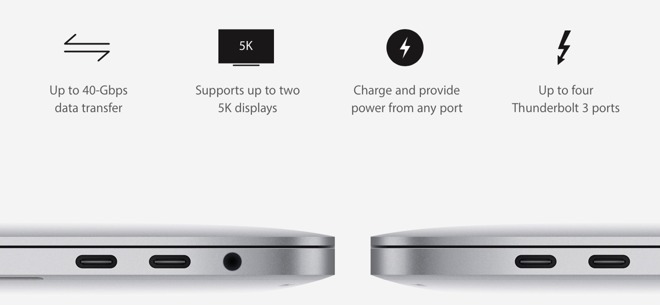
Thunderbolt ports are commonly used for power delivery for MacBooks at the same time as data transfers.
For phone and device chargers, the use of the high-voltage GaN means more power can be transferred at a far higher efficiency than silicon, making them more suitable for this sort of application.
Since more power can be shifted through GaN components, which can also be made more compact than their silicon counterparts, this means that more can be built into the GaN component instead of relying on multiple silicon components, shrinking the amount of components required for a charger, and potentially allowing for the overall size of the charger to be smaller.
To consumers, they can expect GaN chargers to be smaller in stature than current-generation chargers, as well as some that keep the same size but offer the ability to provide power to more devices, as well as being able to charge high-Watt items like MacBooks with ease.
![An example of how small a GaN charger could be against some larger traditional chargers. [via Anker]](https://photos5.appleinsider.com/gallery/31563-53249-GaN-charger-size-comparison-l.jpg)
An example of how small a GaN charger could be against some larger traditional chargers. [via Anker]
The processes to create silicon components are already widely established and reasonably cheap on a per-component basis. GaN is still relatively in its infancy for commercialization, which makes it more expensive to produce than silicon, so until it becomes cost-effective with its benefits to create GaN components, firms lack much of an incentive to switch over.
For the moment, only a few semiconductor vendors are producing GaN components, and it won't be until the major semiconductor fabricators start using the material at a high scale for chips that costs won't reduce.
This means not many charger manufacturers are using GaN as could be, but this is likely to change once the supply and cost become more reasonable. Even so, several companies are taking advantage of the technology's benefits now.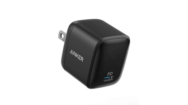
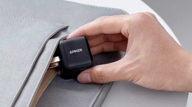
Anker PowerPort Atom PD 1
One major example of how small a GaN charger can get is the Anker PowerPort Atom PD 1. Measuring 1.6 inches by 1.8 inches by 1.5 inches, the compact cube is a 30W USB-C charger that is capable of charging larger devices as well as smaller items.
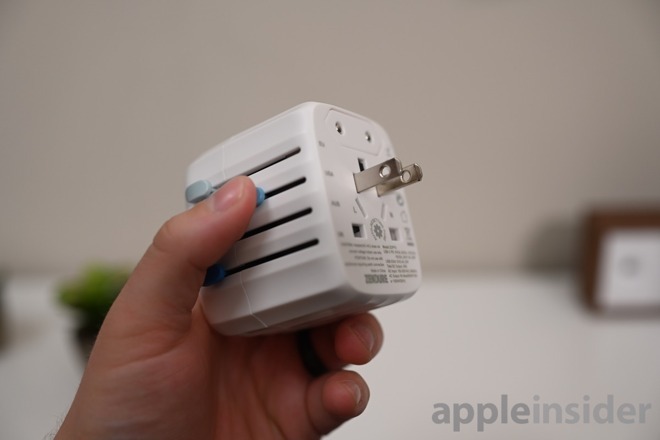
Zendure Passport GO
Recently reviewed by AppleInsider, the Zendure Passport GO is a 30-Watt USB-C charger that takes advantage of GaN's space-saving nature to create an extremely capable adapter. Using four retractable adapters, the charger can work in over 200 countries worldwide, yet retain its small stature.

RAVPower USB-C 45W GaN Wall Charger
For those wanting more wattage, the RAVPower USB-C 45W GaN Wall Charger is capable of recharging a 12-inch MacBook in two hours. To help with travel, the prongs can be folded away into its thin 0.59-inch body, with its sensing capability able to switch between five output levels to optimally charge the device.
What is Gallium Nitride?
Gallium nitride, also referred to as GaN, is a semiconductor that can be used to produce chips for electronics, in a similar manner to silicon. GaN is a transparent crystalline material, often used in the production of LEDs for the last 30 years, with its high frequency capabilities allowing for the production of violet laser diodes.While silicon is the main material used for chip production, the limits of its properties relating to thermal and electrical transfer means it is getting harder for chip producers to work with it. As the race for smaller chip production processes intensifies, at some point the producers will have to look to other materials that could be used for processor creation in different ways.
A gallium nitride crystal [via Wikipedia]
GaN is the current best candidate to take over from Silicon, primarily for its "band gap" efficiency. The "band gap" refers to how a material can conduct electricity, with a wider band gap allowing for higher voltages to be used without issue.
What are its benefits over silicon?
In the case of GaN, its band gap is considerably higher than silicon, meaning it is capable of conducting far higher voltages over time. The bigger band gap also means that current is able to pass through a chip made form GaN faster than Silicon, which in turn could lead to even faster processing.The band gap efficiency can manifest benefits in a number of other ways than processing speed. For example, as it is easier for energy to pass through, less power is needed to use a GaN-powered chip to offer similar benefits.
The efficiency also means the chips could be constructed smaller due to minimal energy loss, such as the case when a processor gets hot under load. This could mean more could be squeezed into the footprint of a silicon processor, or the footprint could be cut down in size, saving on material in its production and possibly physical size.
The higher voltage capacity also lends itself well to systems involving power transfers, such as chargers, while the ability to operate at higher temperatures could allow for components using it to be mounted in places where heat isn't as much of an issue.
What does this have to do with chargers?
At their simplest, a charger applies a current to a battery in an attempt to reverse a chemical reaction inside each one. While early chargers applied a charge constantly without monitoring the battery itself, potentially leading to overcharging and damaging the battery, later versions include monitoring systems that can vary the current down over time, minimizing the possibility of overcharging.Modern chargers as well as hardware which provides "power delivery" to other items, such as Thunderbolt docks or monitors providing power to a MacBook, sometimes provide considerable amounts of power to the device. For chargers with "fast charging" capabilities, this can give a battery in a smartphone half of its capacity in terms of available power in a short space of time, before reverting to lower current levels as it gets fuller.
Thunderbolt ports are commonly used for power delivery for MacBooks at the same time as data transfers.
For phone and device chargers, the use of the high-voltage GaN means more power can be transferred at a far higher efficiency than silicon, making them more suitable for this sort of application.
Since more power can be shifted through GaN components, which can also be made more compact than their silicon counterparts, this means that more can be built into the GaN component instead of relying on multiple silicon components, shrinking the amount of components required for a charger, and potentially allowing for the overall size of the charger to be smaller.
To consumers, they can expect GaN chargers to be smaller in stature than current-generation chargers, as well as some that keep the same size but offer the ability to provide power to more devices, as well as being able to charge high-Watt items like MacBooks with ease.
An example of how small a GaN charger could be against some larger traditional chargers. [via Anker]
Why are we still using older charging technology?
In short, money.The processes to create silicon components are already widely established and reasonably cheap on a per-component basis. GaN is still relatively in its infancy for commercialization, which makes it more expensive to produce than silicon, so until it becomes cost-effective with its benefits to create GaN components, firms lack much of an incentive to switch over.
For the moment, only a few semiconductor vendors are producing GaN components, and it won't be until the major semiconductor fabricators start using the material at a high scale for chips that costs won't reduce.
This means not many charger manufacturers are using GaN as could be, but this is likely to change once the supply and cost become more reasonable. Even so, several companies are taking advantage of the technology's benefits now.
What GaN chargers are available right now?
Anker PowerPort Atom PD 1
One major example of how small a GaN charger can get is the Anker PowerPort Atom PD 1. Measuring 1.6 inches by 1.8 inches by 1.5 inches, the compact cube is a 30W USB-C charger that is capable of charging larger devices as well as smaller items.
Zendure Passport GO
Recently reviewed by AppleInsider, the Zendure Passport GO is a 30-Watt USB-C charger that takes advantage of GaN's space-saving nature to create an extremely capable adapter. Using four retractable adapters, the charger can work in over 200 countries worldwide, yet retain its small stature.
RAVPower USB-C 45W GaN Wall Charger
For those wanting more wattage, the RAVPower USB-C 45W GaN Wall Charger is capable of recharging a 12-inch MacBook in two hours. To help with travel, the prongs can be folded away into its thin 0.59-inch body, with its sensing capability able to switch between five output levels to optimally charge the device.
Comments
As noted, it's not either, but there are other things to consider in that image. For instance, the thickness of the Anker charger compared to Apple's charger, not shown in that particular image, and that the Anker charger seems to be enlarged quite a bit when you compare the AC plug prongs for each one. Regardless of what you see in the image the takeaway from the article is that GaN has clear benefits for consumers.
As a geologist there are some inconsistencies in these numbers, such as not all bauxite has recoverable Gallium and because of its unique low melting nature it cannot be uniquely certified as to quality like a gold bar for example (its difficult to trace and susceptible in electronics to contamination).
GaN works in some electrical applications, such as the chargers note, but it would be difficult to scale as chip sets (about 10 years ago Ga Arsenides were contenders to supplant silicon). There are some really exciting programs looking at high temp superconductors, light based chipsets and quantum effects that will most likely be the best candidate to take over silicon in the future.
On the flip flip side GaN has been making significant progress in power electronics. This is a big advantage in chargers if you are willing to pay for it.
High or low melting point? Did you contradict yourself between the first and second paragraphs?
I’m still interested in comparisons of GaN, in terms of environmental impact and availability, in comparison to existing materials used. There are many rare materials slowly being exhausted by this industry, and also many which cause great environmental harm to extract and process. Almost never does that seem to come into the conversations about new tech.
Firstly, it refers to GaN "chips" implying that it's being used here for integrated electronics (i.e. a single die containing multiple transistors, like a microprocessor), but that's not what's happening. These chargers are using established switched-mode power converter topologies and replacing silicon (Si) MOSFETs (Metal-Oxide-Semiconductor Field-Effect Transistors, a Si die consisting of a single transistor, that is able to handle lots of voltage and current, relative to a microprocessor transistor) with GaN HEMTs (High-Electron-Mobility Transistors).
Secondly, it refers to voltage being "conducted". Power transistors do not "conduct" voltage. In power converters like these, the power transistors operate in a "switched mode", being either "off", or "fully" on (where they behave like a very small resistance in the tens of milliohms range). When "on", they conduct current, and when "off" they block voltage.
When conducting, the power transistor dissipates some power (referred to as "conduction loss"), this being equal to the current squared multiplied by the resistance. So, lower resistance = lower losses. However, when making the transistor, there is a tradeoff between how many volts the transistor can block when off, and how low its resistance is. The more volts you need to block (in the case of these power converters, the transistors are usually rated at around 600 V to 650 V), the higher the resistance. The wide bandgap of GaN gives a better tradeoff between voltage blocking capability and on-resistance, compared to Si. Additionally, when transitioning from "on" to "off" or visa-versa, there is a brief period of very high power dissipation in the transistor (referred to as "switching loss"). Crudely speaking, the faster a transistor can perform these transitions, the lower the switching loss will be. GaN power transistors are much faster than Si devices and the switching losses are much smaller.
At a very basic level, switching power converters operate by taking small packets of energy from the source (in this case a mains/grid connection), storing that energy temporarily, and then outputting that energy to the load. The energy is stored internally in inductors and capacitors, and routed/transferred with power transistors and transformers. How often the packets of energy are routed around is referred to as the switching frequency. The higher the switching frequency, the smaller the energy storage components and transformers can be. However, as mentioned previously, each time a transistor transitions from "on" to "off" or visa versa, it wastes some energy as heat. So the higher the switching frequency, the higher the losses. If in each transition you lose less heat, you can afford to increase the switching frequency and therefore make the inductors, capacitors, and transformers in your power converter smaller.
In summary, the key benefits of GaN over Si, when it comes to power transistors, are:
A better tradeoff between on-state resistance and blocking voltage (lower conduction loss)
Much faster switching transitions leading to lower switching losses, allowing a higher switching frequency.
Now, both GaN and Si transistors have an upper limit of temperature that they can safely operate at, typically 150 C or 175 C. Any power dissipation in the transistor is converted to heat, which must be extracted by a cooling system to keep the transistor below the maximum allowed limit. If you've less heat to extract (due to lower losses), you can make the cooling system smaller. So, there's two ways that the power converter can be made smaller:
1. Get the losses down so the cooling system can shrink
2. Increase the switching frequency to make the inductors, capacitors, and transformers smaller
When compared to power converters using Si transistors, a GaN-based one will be using a mixture of these two approaches.
GaN transistors are also smaller than Si ones, but the impact of that is fairly minimal relative to the other effects outlined above.
To learn more, you can get a free book on power electronics here (registration is required, but free). For the avoidance of doubt, I am not Barry Williams.
Silicon have a very particular crystalline structure that has been maintained its edge on electronic devices for about fifty years now (and many potential contenders). For those who remember, the first integrated circuit was made of germanium, then, the semiconductor of choice.
We are soon hitting a hard wall in our capability to lower the size of electronics, and even at that, silicon is our best bet, due to its small crystalline lattice constant of just 0.54 nanometers. That ought to give the industry about another ten-fold decrease in size, as technology goes forward. GaN lattice constant is 0.52 nanometers, which is smaller, but that won’t lead very far ahead.