TSMC on schedule for 3nm Apple 'A16' iPhone and iPad chip in 2022

Posted:
in General Discussion
Apple manufacturing partner TSMC is on track to start producing chips using a 3nm chip fabrication process in late 2022, and is already working on improved 5nm processes.


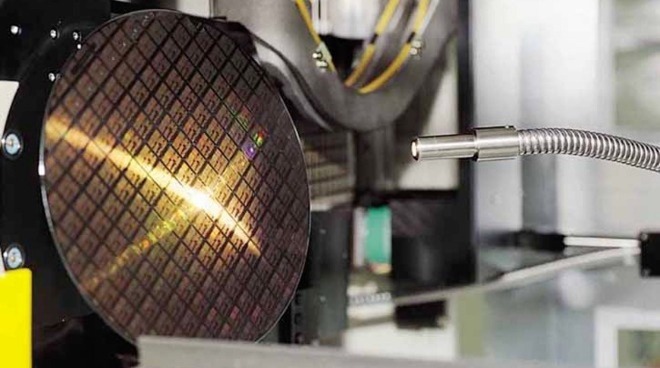
Like other chip makers, TSMC has been working to develop processes at smaller nanometer levels, with some of its research going into creating 3-nanometer production processes. At that level, it is claimed TSMC has started to construct production lines and related facilities for creating 3-nanometer chips.

The 3-nanometer project is still on schedule, according to DigiTimes, with risk production anticipated to take place in 2021 followed by volume production in the second half of 2022. If accurate, and based on typical iPhone production schedules, this could lead to the Apple-designed A15 at the absolute earliest or more realistically, the A16 chip in 2022 using the process.

For the more immediately accessible 5-nanometer chips, TSMC is said to be in volume production with the technology, but it is already working on improved versions. The company is said to be creating more processor variants, including a further-enhanced 5nm node that expands on the existing 5nm Plus node.

It is thought Apple is using TSMC's 5nm processes to create the next generation of A-series chips destined for the "iPhone 12" tentatively titled the "A14," with production scheduled for mid-2020. In April, it was reported Apple increased its chip order for the fourth quarter of 2020, potentially due to an anticipated higher demand for the annual iPhone refresh.

TSMC is also intending to move some of its chip production to the United States, in a factory in Arizona thought to cost $12 billion. It Is far from operational, with construction commencing in 2021 and chip production expected to start in 2024, but it offers the prospect of some A-series chips being made on US soil.

Comments

  • Reply 1 of 16
    thttht Posts: 5,441member
    TSMC is a huge reason why Apple is going all in on their own ARM chips in all their products. Always encouraging to see progress towards the next node.
    jony0watto_cobra
  • Reply 2 of 16
    prismaticsprismatics Posts: 164member

    This fab is almost like the Foxconn thing. A fab this small and with technology that will be that old when the factory starts production is meaningless in the global scope.

  • Reply 3 of 16
    bageljoeybageljoey Posts: 2,004member
    Holy cow!  5nm to 3nm?  A 40% size reduction in 2 years?  That’s is just crazy. 

    (I always go back to a paper I wrote in college where it was stated with complete certainty that 100nm was the smallest transistor size theoretically possible, but that 200nm was probably the practical limit. 
    Moore’s Law was doomed. DOOMED!)
    netroxking editor the grateJWSCCloudTalkinjony0watto_cobraDAalseth
  • Reply 4 of 16
    SpamSandwichSpamSandwich Posts: 33,407member
    “DigiTimes”... say no more. SMDH.
  • Reply 5 of 16
    netroxnetrox Posts: 1,421member
    How is it even remotely possible? How do they deal with thermal noise and leakage? 


    watto_cobra
  • Reply 6 of 16
    avon b7avon b7 Posts: 7,667member

    This fab is almost like the Foxconn thing. A fab this small and with technology that will be that old when the factory starts production is meaningless in the global scope.

    The technology ages very well but it won't be used for cutting edge scenarios. There will be demand for it. Last year it was basically Huawei and Apple sucking up TSMC capacity at launch while others waited in line for their designs to be built this year and beyond. Whether it is cost effective or not to use the chips made in the U.S fab might be an issue. That's an accounting matter, though. Subsidies are likely to be an important factor.

    Someone may even try to pass laws ensuring fabrication on U.S soil for 'security' reasons. 
    prismatics
  • Reply 7 of 16
    lkrupplkrupp Posts: 10,557member
    Yawn... let me know when they get to 0nm
    SpamSandwichjony0
  • Reply 8 of 16
    anomeanome Posts: 1,533member
    I'm starting to wonder if "nm" is becoming like GHz - formerly useful but increasingly meaningless as a performance measure. Are we actually using wires/channels/whatever 3nm wide? Because that's at a point where actually pinning down the location of an electron gets kind of dodgy. There is a hard limit somewhere around here where it ceases to be functional.
    JWSCnetroxwatto_cobra
  • Reply 9 of 16
    JWSCJWSC Posts: 1,203member
    bageljoey said:
    Holy cow!  5nm to 3nm?  A 40% size reduction in 2 years?  That’s is just crazy. 

    (I always go back to a paper I wrote in college where it was stated with complete certainty that 100nm was the smallest transistor size theoretically possible, but that 200nm was probably the practical limit. 
    Moore’s Law was doomed. DOOMED!)
    Crazy is what I was thinking too. But if they can pull it off, wow!

    WRT logic and data integrity, it is possible that they will design redundancy into the architecture. If two out of 3 agree then proceed, and damn the “minority report.” With the physical space savings you could afford the redundancy. What that means for the number of steps in the processing cycle and possibly even clock speed I couldn’t guess. Way beyond my areas of expertise.
    watto_cobra
  • Reply 10 of 16
    thttht Posts: 5,441member
    anome said:
    I'm starting to wonder if "nm" is becoming like GHz - formerly useful but increasingly meaningless as a performance measure. Are we actually using wires/channels/whatever 3nm wide? Because that's at a point where actually pinning down the location of an electron gets kind of dodgy. There is a hard limit somewhere around here where it ceases to be functional.
    “nm“ has been foundry marketing since 22 nm or so. Numbers from different companies can’t be compared directly. But if you are mindful of the transistor densities at each node per foundry, you get used to it.

    Grossly, TSMC 10nm = Intel 14nm, TSMC 7nm = Intel 10nm, TSMC 5nm = Intel 7nm. 

    Issue is Intel’s 10nm has been broken for the past 3 years and only produces low power mobile chips, and only for the past 9 months at that. The high power laptop chips and desktop chips won’t be fabbed on their 10nm fab until 2021, probably late 2021. Who knows really. 

    If Apple has TSMC 5nm chips in 2021, those chips will outperform Intel’s and they are in front of AMD in TSMC’s queue. When the iPhone ships this Fall with the 5nm A14, it will increase the iPhone’s lead in single core performance across all of Apple’s products, including the desktops. 

    The issues with quantum tunneling have been mitigated by making the channels/gates taller. So the transistors are getting smaller on the 2D footprint, but are adding more material vertically, reducing quantum tunneling. They look like fins and every foundry uses this type of design and brands their process as FinFET something or the other. 

    Anyways, if Apple had its Kwisatz Haderach hat on, they should have transitioned to ARM in 2017 or 2018 when TSMC 10nm first came out. 
    JWSCanomeentropyswatto_cobraDAalsethjdb8167
  • Reply 11 of 16
    SpamSandwichSpamSandwich Posts: 33,407member
    lkrupp said:
    Yawn... let me know when they get to 0nm
    Next up, Angstroms.
    jony0watto_cobra
  • Reply 12 of 16
    entropysentropys Posts: 4,166member
    lkrupp said:
    Yawn... let me know when they get to 0nm
    Or at least one ludicrumeter.
    watto_cobra
  • Reply 13 of 16
    entropysentropys Posts: 4,166member
    tht said:
    anome said:
    I'm starting to wonder if "nm" is becoming like GHz - formerly useful but increasingly meaningless as a performance measure. Are we actually using wires/channels/whatever 3nm wide? Because that's at a point where actually pinning down the location of an electron gets kind of dodgy. There is a hard limit somewhere around here where it ceases to be functional.
    “nm“ has been foundry marketing since 22 nm or so. Numbers from different companies can’t be compared directly. But if you are mindful of the transistor densities at each node per foundry, you get used to it.

    Grossly, TSMC 10nm = Intel 14nm, TSMC 7nm = Intel 10nm, TSMC 5nm = Intel 7nm. 

    Issue is Intel’s 10nm has been broken for the past 3 years and only produces low power mobile chips, and only for the past 9 months at that. The high power laptop chips and desktop chips won’t be fabbed on their 10nm fab until 2021, probably late 2021. Who knows really. 

    If Apple has TSMC 5nm chips in 2021, those chips will outperform Intel’s and they are in front of AMD in TSMC’s queue. When the iPhone ships this Fall with the 5nm A14, it will increase the iPhone’s lead in single core performance across all of Apple’s products, including the desktops. 

    The issues with quantum tunneling have been mitigated by making the channels/gates taller. So the transistors are getting smaller on the 2D footprint, but are adding more material vertically, reducing quantum tunneling. They look like fins and every foundry uses this type of design and brands their process as FinFET something or the other. 

    Anyways, if Apple had its Kwisatz Haderach hat on, they should have transitioned to ARM in 2017 or 2018 when TSMC 10nm first came out. 
    Liked for the Dune reference.and ‘cause informative too.
  • Reply 14 of 16
    jdb8167jdb8167 Posts: 626member
    anome said:
    I'm starting to wonder if "nm" is becoming like GHz - formerly useful but increasingly meaningless as a performance measure. Are we actually using wires/channels/whatever 3nm wide? Because that's at a point where actually pinning down the location of an electron gets kind of dodgy. There is a hard limit somewhere around here where it ceases to be functional.
    It really doesn’t matter what the nm value is. What matters is that transistor density is increasing. 

    A10 2016 16 nm: 3.3 billion transistors @ 125 mm^2

    A11 2017 10 nm: 4.3 billion transistors @ 87.66 mm^2

    A12 2018 7 nm: 6.9 billion transistors @ 83.27 mm^2

    A13 2019 7 nm: 8.5 billion transistors @ 98.48 mm^2

    The comparison between the A12 vs. the A13 is instructive. The node size stayed at 7 nm and in order to increase the number of transistors the die size had to increase 18% to get a 23% increase in total transistors where previous generations actually reduced the die size for more transistors. 
  • Reply 15 of 16
    apple using 3nm in 2022 will be a big leap and will be far ahead of its rivals and 2nm in 2024(if possible), I wonder what will happen after that ? will they scale up the dye size or will some breakthrough happen?
  • Reply 16 of 16
    Can't wait to see them finish compared to Tesla of Elon Musk Project Titan: Apple Car Develop Chips for Self-Driving Cars with TSMC https://techoslava.com/2020/12/project-titan-apple-car-develop-chips-for-self-driving-cars-with-tsmc/
Sign In or Register to comment.