M4 iPad Pro teardown shows copper logo, highly repairable internals

A teardown of the 13-inch iPad Pro with M4 reveals it is a fairly repairable tablet, as well as an actual practical use for the rear Apple logo.
![Mid-teardown of the 13-inch iPad Pro with M4 [Youtube/Phone Repair Guru]](https://photos5.appleinsider.com/gallery/59712-122041-teardownphonerepairguru1-xl.jpg)
Mid-teardown of the 13-inch iPad Pro with M4 [Youtube/Phone Repair Guru]
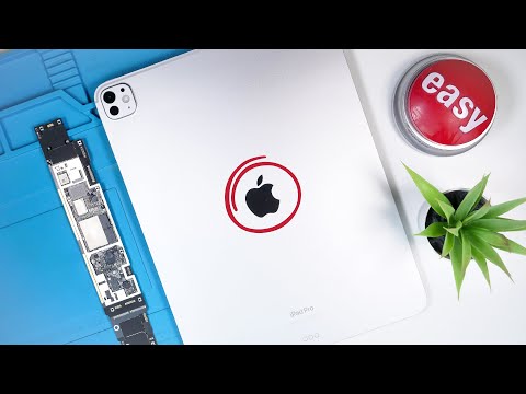
In between videos of YouTubers bending Apple's new hardware for clicks, there are some that try to offer more constructive criticism. In the case of one teardown, it shows Apple's latest iPad Pro to be quite repairable, and with some interesting changes.
The teardown by Phone Repair Guru published early on Friday follows the usual pattern of events to take apart the iPad Pro. However, there was an initial fear of things going wrong, after heating up the iPad Pro made it fairly flexible.
The screen was removed using a typical suction cup and plastic card to loosen the adhesive keeping the screen in place. Once the last cables were removed, it allowed full access to the internal components.
A collection of flex cables fed from the Tandem OLED screen to the middle of the inside, with the main circuit board of the iPad acting as a spine. A copper tape's removal exposed the chips in the middle, including the centrally-located M4 chip.
Screws were used to hold in the camera assemblies, along with a small amount of glue. Just three screws held in the USB Type-C port, which certainly helps with repairability.
![The uncovered mainboard of the iPad Pro with M4 [Youtube/Phone Repair Guru]](https://photos5.appleinsider.com/gallery/59712-122044-teardownphonerepairguru1-3-xl.jpg)
The uncovered mainboard of the iPad Pro with M4 [Youtube/Phone Repair Guru]
Two battery panels flank the chip spine, with pull tabs used to eliminate the adhesive between each battery cell and the back casing.
"Assuming everything on here isn't serialized to oblivion, this device is pretty repairable," the YouTuber complimented, on what was deemed an "enjoyable" teardown experience.
After removing the glued-down board, tearing through some graphite paper revealed the Apple logo. Further scraping away at the icon confirmed that it contains copper.
![The Apple logo, scratched to show copper [Youtube/Phone Repair Guru]](https://photos5.appleinsider.com/gallery/59712-122042-teardownphonerepairguru1-2-xl.jpg)
The Apple logo, scratched to show copper [Youtube/Phone Repair Guru]
The copper Apple logo is actually beneficial to the iPad's running. Due to its positioning alongside the main M4 chip, it can act as a heat sink to reduce temperatures.
Read on AppleInsider
Comments
So, that heat spreader between the top of the SoC and the display is doing most of the work, imo. The copper-alloy logo? Probably does do something, but not a lot.
Apple's thermal dissipation strategy for their passively cooled machines is to spread out the heat from the SoC to as large a surface area as possible. They don't want concentrated hot spots on the surface of the machine. That's what the graphene layered metallic shield does: spreads out the heat to a large surface area.