A20 chip developments could mean more iPhone variants in 2026

Jump to First Reply
Posted:
in Future Apple Hardware

A change in the way TSMC makes chips for Apple could mean a lot more variation in performance for the iPhone 18 models, by Apple switching combinations of CPU, GPU, and Neural Engine.

Colorful semiconductor wafers with intricate rectangular patterns, reflecting vivid hues of green, yellow, and blue, showcasing microchip design.
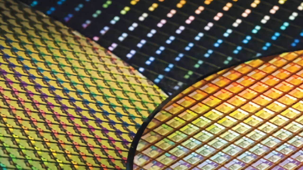
Dies on wafers - Image credit: TSMC


One of the problems with chip production is that manufacturers are usually locked into a few specific chip designs, due to the expense and difficulty of creating each one. However, using a new technique will potentially allow TSMC to provide Apple with far more flexibility than ever before.

According to analyst Ming-Chi Kuo on Tuesday, Eternal Materials has been named as an advanced packaging materials supplier to TSMC. Eternal will become the only supplier of the liquid molding compound (LMC) and molding underfill (MUF), used to encapsulate chips, for Apple's 2026 iPhone and Mac chip generations.

The order from Eternal effectively confirms a claim from October 2024 that TSMC will be using a new technique to make Apple's chips in a more flexible way.

Ming-Chi Kuo has a very good record when it comes to Apple-related claims. The accuracy of the supply chain checks are his strong suit, such as stories like this about supplier changes.

From InFO to WMCM


Chip packaging refers to a way to set up the chip's die, as well as encapsulating it. The process also prepares the chip to communicate with other components on a circuit board, such as the components of an iPhone.

InFO (Integrated Fan-Out), the current technique, is used because Apple's non-CPU components are integrated into the chip package. That is, memory is added to the chip package directly instead of being an external component, improving memory performance overall.

The technique works well because Apple is using a single die housing the CPU, GPU, and the Neural Engine, and limited memory configurations. WMCM (Wafer-level Multi-Chi Module) is a different packaging technique that is better suited for a wider number of configurations.

WMCM is capable of putting together multiple dies into a single package, one that is still small enough for Apple's purposes. By using WMCM, Apple can have separate dies for the CPU, the GPU, and the Neural Engine, Apple can better mix and match the combinations of each, increasing the number of different chip configurations it could produce.

This can be imagined by using one CPU, GPU, and Neural Engine for chips destined in a Pro-tier iPhone, but then switching the GPU for one with more cores for use as an M-series chip. Apple could also differentiate the chips between the A20 and A20 Pro further by adding more powerful dies to one package, and using different sets for the other, while still using the same CPU.

Rumor Score: Possible

Read on AppleInsider

Comments

  • Reply 1 of 7
    melgrossmelgross Posts: 33,725member
    How would this work with Apple’s fast fabric connection scheme? Right now, the RAM is not on chip, but is connected to the fabric.
     0Likes 0Dislikes 0Informatives
  • Reply 2 of 7
    thttht Posts: 6,033member
    [InFO] technique works well because Apple is using a single die housing the CPU, GPU, and the Neural Engine, and limited memory configurations. WMCM (Wafer-level Multi-Chip Module) is a different packaging technique that is better suited for a wider number of configurations. WMCM is capable of putting together multiple dies into a single package, one that is still small enough for Apple's purposes. By using WMCM, Apple can have separate dies for the CPU, the GPU, and the Neural Engine, Apple can better mix and match the combinations of each, increasing the number of different chip configurations it could produce.
    This explanation could use work. It doesn’t make much sense. 

    I actually can’t find out what WMCM is. Seems like it is an initialism exclusive to Kuo, and he is not using TSMC’s terms of art?

    Apple has been using a variant of TSMC’s InFO for 6 or 8 years now. They’ve been doing package-on-package for iPhone SoCs where the DRAM package sits on top of the SoC, and the connections from the DRAM to the memory controller in the SoC, which at the edge of the SoC. The I/O connections are “fanning out” out of the edge of the chip, as opposed to at the bottom through the typical pins or balls that you see in chip packaging. 

    In M SoCs, since there are upwards of 8 DRAM packages, they aren’t stacked on top of the SoC, but are adjacent to the edges of the chip. 

    For WMCM, it appears to be a variant of TSMC’s wafer-on-wafer or wafer-in-silicon packaging (CoWoS). This is an advancement on silicon interposers. There is a silicon wafer that serves as an ultra-dense I/O substrate, enabling near chip-level bandwidths. This allows discrete CPU, GPU, NPU, cache to be mounted on it and not have a big interconnection slowdown. 

    It’s what you see for GPUs and AI accelerators using HBM memory, which requires a whole lot of connections. There are also variants with such as silicon bridges which is just a small edge sized chip that connects two chips, instead of a “big” wafer or silicon chip that all the logic and memory chips are mounted on. 

    Silicon interposers are expensive. It’s another chip in the package. The only reason, imo, Apple would use it is that prices at TSMC’s N2 node are acceptable, or, they have no choice. 
    appleinsideruserroundaboutnow
     1Like 0Dislikes 1Informative
  • Reply 3 of 7
    thttht Posts: 6,033member
    melgross said:
    How would this work with Apple’s fast fabric connection scheme? Right now, the RAM is not on chip, but is connected to the fabric.
    RAM will be off chip, but in-package as seen for several years now. Apple is going to be using mass market LPDDR memory. So, they may be mounted on a wafer or a silicon bridge, but they are still are connected to a memory controller. This memory controller may be its own chip and connected to the fabric bus connecting all the other chips and cache, but it is still LPDDR memory. 

    Memory won’t be faster. Apple’s advantage is being able to use upwards of 16 (32?) channels of LPDDR versus Intel and AMD who use 2 to 8 channels, most commonly 4 I believe. So, lots of bandwidth on Pro and Max SoCs. 

    There are rumors of special wide I/O chips, but you should be skeptical of that. 
    roundaboutnow
     0Likes 0Dislikes 1Informative
  • Reply 4 of 7
    mattinozmattinoz Posts: 2,695member
    Why would they create compute modules each with cpu, gpu and npu cores?

    that would give the processes running on each module full speed access between cores.  Then pack the same modules in different configurations to make the whole M family use the connecting module as the platform hub that has all the single and device specific functions 
     0Likes 0Dislikes 0Informatives
  • Reply 5 of 7

    I thought they always taught in the school of journalism to define your terms...(?)

    Taiwan Semiconductor Manufacturing Company (TSMC)


    williamlondon
     0Likes 1Dislike 0Informatives
  • Reply 6 of 7
    mattinozmattinoz Posts: 2,695member

    I thought they always taught in the school of journalism to define your terms...(?)

    Taiwan Semiconductor Manufacturing Company (TSMC)


    But its proper initialism not a common initialism. Would you expect them to write Bob (Robert Allen Zimmerman) if talking about the bio pic?
    williamlondon
     1Like 0Dislikes 0Informatives
  • Reply 7 of 7
    melgrossmelgross Posts: 33,725member
    tht said:
    [InFO] technique works well because Apple is using a single die housing the CPU, GPU, and the Neural Engine, and limited memory configurations. WMCM (Wafer-level Multi-Chip Module) is a different packaging technique that is better suited for a wider number of configurations. WMCM is capable of putting together multiple dies into a single package, one that is still small enough for Apple's purposes. By using WMCM, Apple can have separate dies for the CPU, the GPU, and the Neural Engine, Apple can better mix and match the combinations of each, increasing the number of different chip configurations it could produce.
    This explanation could use work. It doesn’t make much sense. 

    I actually can’t find out what WMCM is. Seems like it is an initialism exclusive to Kuo, and he is not using TSMC’s terms of art?

    Apple has been using a variant of TSMC’s InFO for 6 or 8 years now. They’ve been doing package-on-package for iPhone SoCs where the DRAM package sits on top of the SoC, and the connections from the DRAM to the memory controller in the SoC, which at the edge of the SoC. The I/O connections are “fanning out” out of the edge of the chip, as opposed to at the bottom through the typical pins or balls that you see in chip packaging. 

    In M SoCs, since there are upwards of 8 DRAM packages, they aren’t stacked on top of the SoC, but are adjacent to the edges of the chip. 

    For WMCM, it appears to be a variant of TSMC’s wafer-on-wafer or wafer-in-silicon packaging (CoWoS). This is an advancement on silicon interposers. There is a silicon wafer that serves as an ultra-dense I/O substrate, enabling near chip-level bandwidths. This allows discrete CPU, GPU, NPU, cache to be mounted on it and not have a big interconnection slowdown. 

    It’s what you see for GPUs and AI accelerators using HBM memory, which requires a whole lot of connections. There are also variants with such as silicon bridges which is just a small edge sized chip that connects two chips, instead of a “big” wafer or silicon chip that all the logic and memory chips are mounted on. 

    Silicon interposers are expensive. It’s another chip in the package. The only reason, imo, Apple would use it is that prices at TSMC’s N2 node are acceptable, or, they have no choice. 
    This is what I’ve been wondering about. The issue is complex. Apple always has a cost/performance equation to work on. So far, their fabric has worked out well. If they brought the GPU off the die as well as the RAM, do they need such expensive technologies, or will the method of just bringing more of the fabric out to the sub board suffice? 
     0Likes 0Dislikes 0Informatives
Sign In or Register to comment.