TSMC will use updated 'N7 Pro' 7-nanometer process for 'A13' chip manufacturing

Apple's "A13" processor will use a 7-nanometer process for its production, but chip foundry TSMC is reportedly planning to use a different enhanced process to the current version it has come up with, named "N7 Pro."
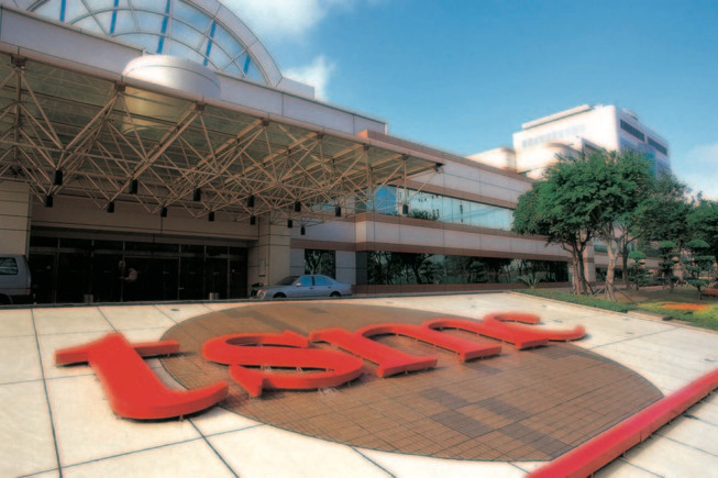
TSMC's offices.
TSMC's use of a 7-nanometer process for the next generation of Apple system-on-chips is not unexpected, with TSMC widely believed to not only continue to be the only supplier of A-series chips in 2019, but also keeping to the same process level. According to one report, TSMC will be making some changes to the process.
The Chinese Commercial Times claims TSMC will move to a 7-nanometer extreme ultraviolet lithography (EUV) process that has the potential for more accurate chip production and more intricate designs, named "N7+." HiSilicon's Kirin 985 chips will be the first to use N7+ in its production, but the Apple-designed "A13" will be the next to go into manufacturing at the firm.
For the A-series chip, TSMC will be bringing out an alternate form of its N7+ process which it calls "N7 Pro." It is unclear exactly what the difference is between N7 Pro and N7+, but it will reportedly be ready for volume production late in the second quarter, in time for A-series production for the fall iPhone refresh.
TSMC has come up with a 5-nanometer design infrastructure that could be used to design future A-series chips and other processors. Current speculation has the "A14" using a 5-nanometer production process for the 2020 iPhones.
Comments
https://semiengineering.com/big-trouble-at-3nm/
... "One chip to rule them all"
http://www.maltiel-consulting.com/Samsung-5nm_No_Limit_to_Silicon_Scaling_maltiel_semiconductor.html
"Samsung is optimistic that EUV double patterning (NA=0.25, 0.32, then 0.6) will take patterning to several nanometers in 2014. His presentation of the fundamental laws of physics (based on Boltzmann distribution and Heisenberg's uncertainty principle) predicts a limit of scaling around 1.2 nm."
Just now they are at 7nm, then 5nm (2020-2021), then 3nm (2022-2023).
There was an experimental transistor made from a single atom (0.1nm):
https://www.sciencedaily.com/releases/2012/02/120219191244.htm
That's the theoretical limit and needed special cooling. Just now performance-per-watt is around 60GFLOP/Watt on 10nm. This allows for 10TFLOPs in average desktops. There's not much practical or commercial need to go beyond 20-30TFLOPs in a personal computer so companies will start to rely more on cloud services over hardware.
For the next 5-6 years they should be able to keep pushing hardware advances as they are now. Then it will level out at typical upgrade cycles and computing hardware will become like other appliances. Computing hardware won't change much at all in design, functionality or performance like refrigerators and televisions but people will keep buying it, just at a slower rate.