Apple shows off the lean, efficient processor lab behind the M3

For the first time, Apple has allowed cameras into one of its processor labs where it tests designs like the M3, while executives explain the firm's approach to building its own chips.
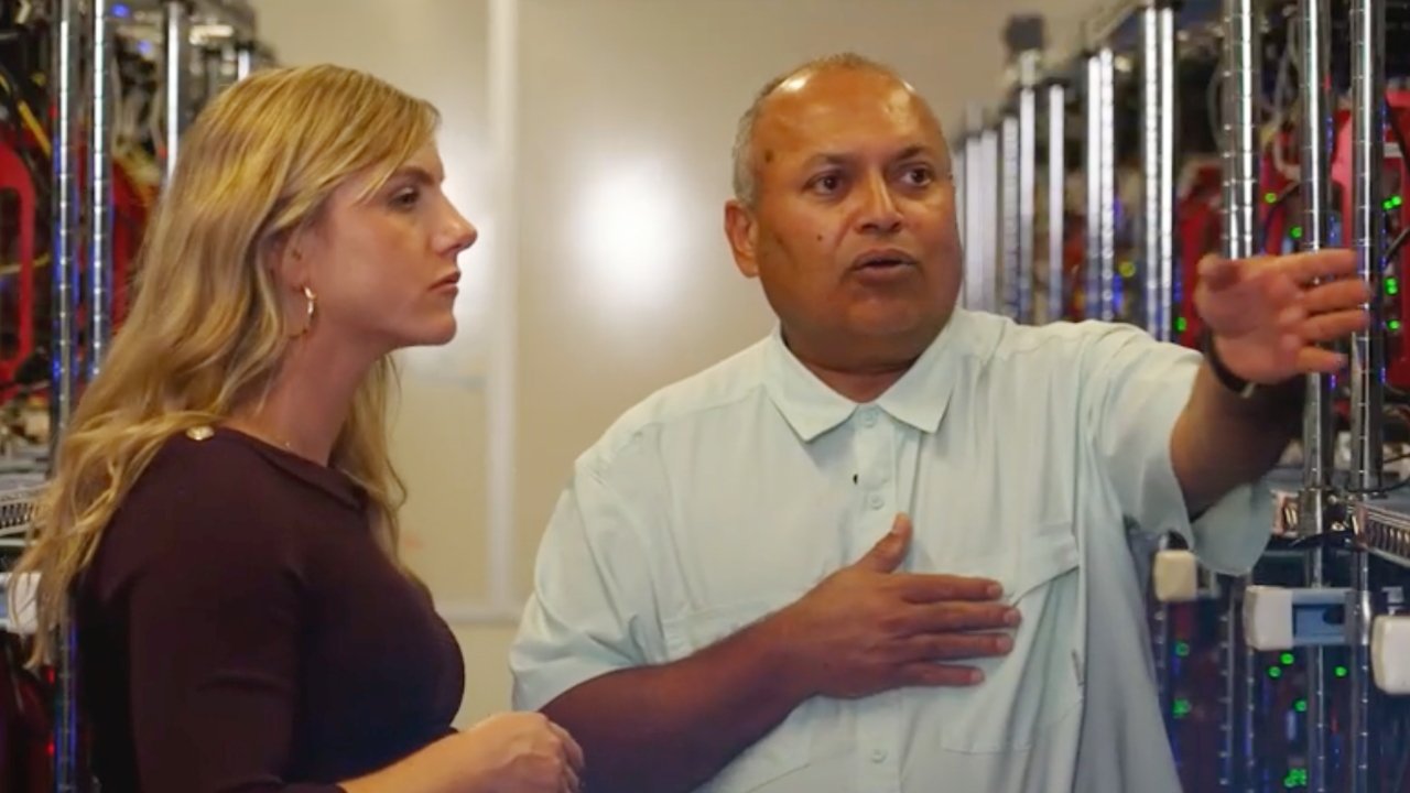
CNBC's Katie Tarasov (left) with Godfrey D'Souza, Apple's senior director hardware validation in a chip lab (Source; CNBC)
One of Apple's many processor labs across the world is in Apple Park, where head of Apple Silicon, Johny Srouji, is based. CNBC was shown what journalist Katie Tarasov described as a "simple room filled with a couple hundred machines, blinking lights, a handful of engineers and lab coats, and a bunch of postage stamp-sized chips being put through rigorous testing."
"I came to Apple [in 2008] with the purpose of building our own silicon for the iPhone," Johny Srouji told CNBC. "It was a very small team at the time, about 40 to 50 engineers, and since then we have grown the team immensely.|
"We have thousands of engineers [now]," he continued. "But if you look at the portfolio of chips we do: very lean, actually. Very efficient."
"Because we're not really selling chips outside, we focus on the product," he said. "That gives us freedom to optimize, and the scalable architecture lets us reuse pieces between different products."
One month after Srouji joined, Apple bought chip company PA Semi for $278 million.
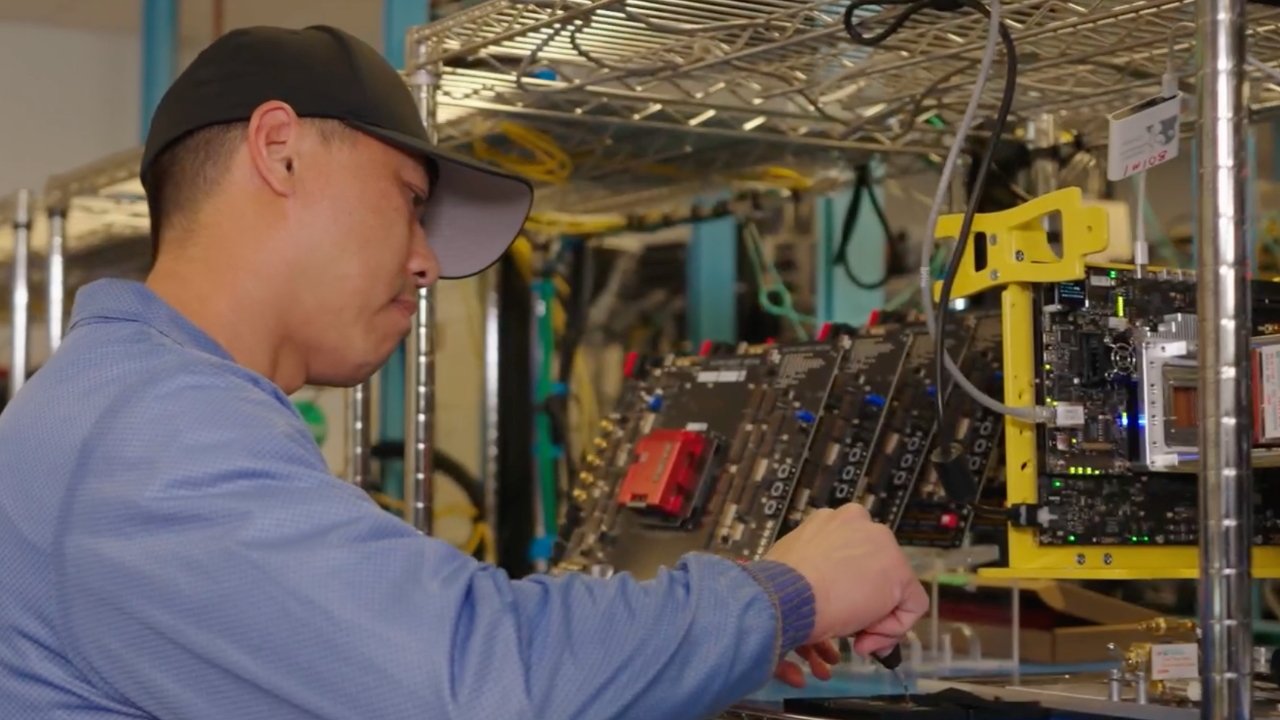
An engineer working in the Apple Park chip lab
Then two years later, Apple launched the A4, its first custom chip for the iPhone 4, and the original iPad. According to Srouji, though, the plan was always to take its processor designs to more products.
"We built what we call the unified memory architecture that is scalable across products," said Srouji. "We built an architecture that you start with the iPhone, but then we scaled it to the iPad and then to the watch and eventually to the Mac."
"We get to design the chips ahead of time," continued Srouji. He says that his staff and those on hardware engineering lead John Ternus, work "to exactly and precisely build chips that are going to be targeted for those products, and only for those products."
"Our aspiration is the product," he said. "We want to build the best products on the planet."
"As a technology team, which also includes the chips in this case," continued Srouji, "we want to build the best technology that would enable that vision."
For the iPhone 15 Pro, Apple announced the A17, and iPhone marketing lead Kaiann Drance says that was "actually the biggest redesign in GPU architecture and Apple Silicon history."
Speaking of the move to Apple Silicon, Ternus told CNBC that "it was almost like the laws of physics had changed."
"All of a sudden we could build a MacBook Air that's incredibly thin and light, has no fan, 18 hours of battery life," he said, "and outperformed the MacBook Pro that we had just been shipping."
"[The new M3 Max MacBook Pro" is 11 times faster than the fastest Intel MacBook Pro we were making," he continued. "And we were shipping that just two years ago."
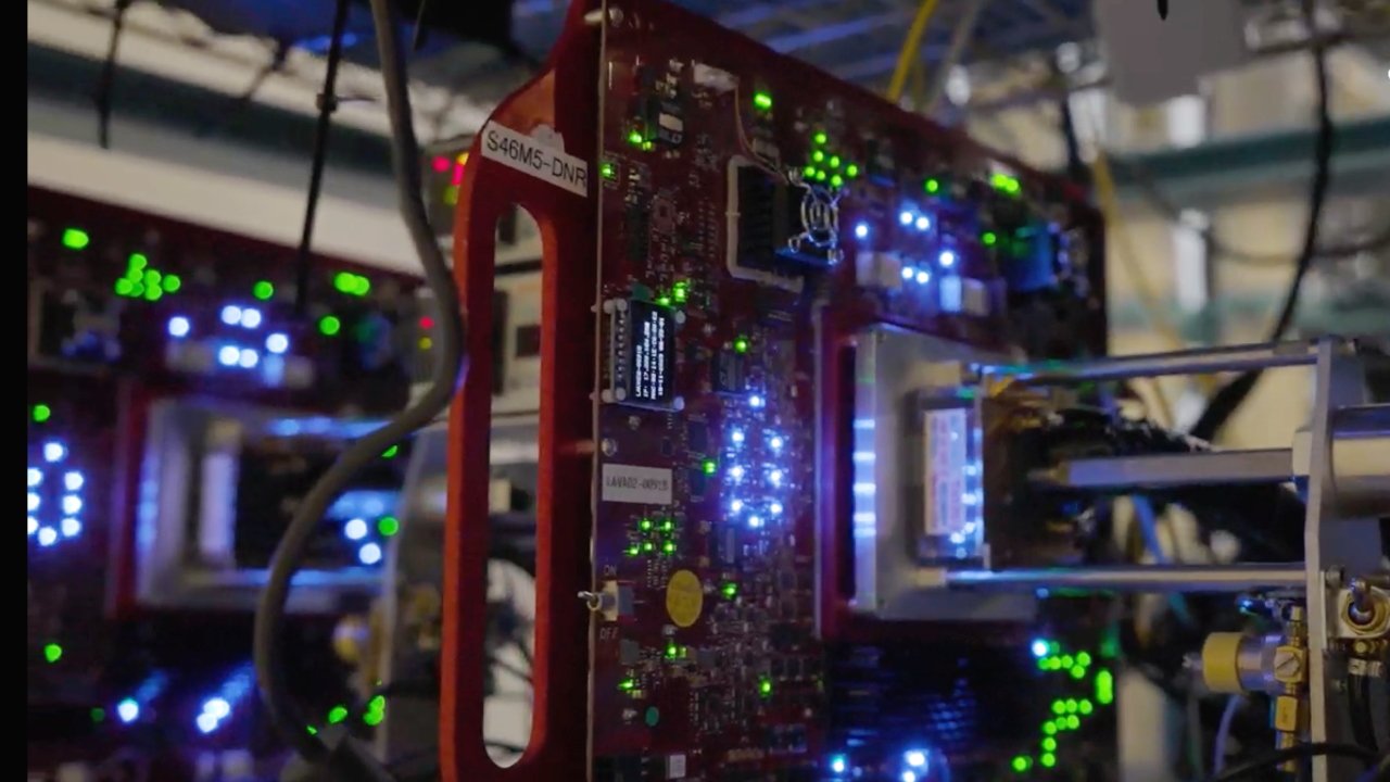
An Apple processor being tested for (among other things) performance under extreme temperatures
The future of processor design
Apple has been reported to be working on its own 5G modem to replace the one it licences from Qualcomm, and at times it has been reported to be having difficulties with it.
Unsurprisingly, Srouji would not comment on Apple's plans for 5G, or any "future technologies and products." However, he said that "we care about cellular, and we have teams enabling that."
In the meantime, despite its own processor labs, Srouji says Apple will "buy off the shelf," if that means its engineers can concentrate "on what really, really matters."
Designing processors for Apple products is one thing, but of course those designs then have to be manufactured. That has long meant working with TSMC, but most recently Apple has announced a partnership with Amkor to take processors and perform chip packaging before they can be added to devices.
Read on AppleInsider

Comments
https://www.bondline.co.uk/blog/the-role-of-esd-lab-coats-in-esd-protected-areas-epas
In any case, here it is: https://www.cnbc.com/2023/12/01/how-apple-makes-its-own-chips-for-iphone-and-mac-edging-out-intel.html (And it's also not too clear at that link either; the image at the top of that article is clickable and will load the video).
"That's not a prism through which you view life, that's a mirror, put it down and step away." ;-)
Of course how that tech is presented and applied will change over time, but it’s been present for a good while now. Apple though, is much more solid, thorough l, and guarded when it comes to just letting the new fad take over their processes and they avoid legal issues, embarrassment, and act as a bastion for proper ethical computing by doing so.
In the past you would see breadboards and test fixtures with all kinds of test instruments like signal analyzers, oscilloscopes, counters, timers, etc., connected to a test fixture (board) with a rats nest of wires and test clips to get the test signals out to the test instruments. Modern systems with VLSI, etc., are way too small and highly integrated to easily attach conventional test instruments to the systems under test. The designers of the chips and SoCs must work closely with those who will be testing the chips to make sure the chip designs provide ways for the chip to be testable.Testability is built into the design. If you imagine a test fixture being bed of nails where each nail is a test point, the chip, package, or board designer must make sure they identify exactly where each test point will be and what signal is associated with the test point. Chips typically have additional circuitry embedded in the chip solely for test purposes.
Product development is far more than the engineering that goes into the design of each component and product as a whole. It must also provide mechanisms to properly test and cost effectively manufacture each component and the product as a whole, not to mention how teh product fits into a larger system or ecosystem. A lot of these essential product development activities go unnoticed by the end consumer of a product. But no product would ever make it into a consumer’s hands without these activities taking place with high degrees of quality and precision.
Also, I'm pretty sure the caption on this photo is wrong; that's not Srouji.